Battery Budgeting for a 0.39-Inch 1080p Micro OLED Near-Eye Display
A 0.39-inch 1920x1080 Micro OLED panel has no backlight rail, so budgeting it like a small TFT module is the fastest way to miss a wearable's runtime target. The pixels are emissive, which means display current follows the image: a dark interface draws a fraction of what a full-white field draws at the same brightness. What genuinely needs engineering attention is the rest of the chain - the MIPI link carrying 1080p, the I2C channel used for configuration, and the difference between a blanked frame and a viewer that is truly asleep. Estimate those as separate line items and you get a number worth designing against; treat the panel as one datasheet figure and the first worn prototype will surprise you. The sections below split the budget, itemise what each standby state still consumes, and describe a bench method that produces a defensible current figure.
Key takeaways
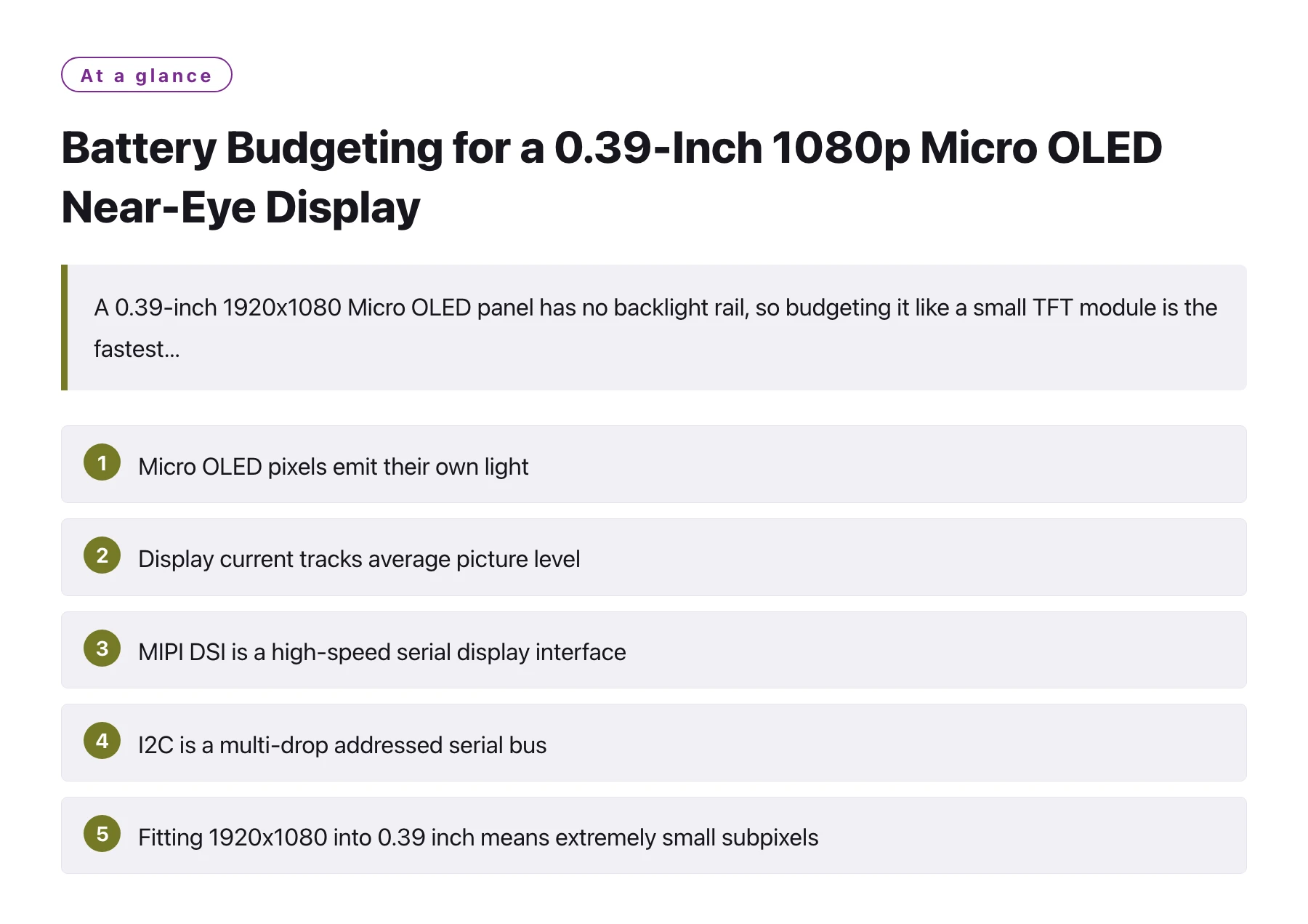
- Micro OLED pixels emit their own light, so the module contains no backlight assembly and adds no LED boost driver or lamp dimming stage to the power tree. [1]
- Display current tracks average picture level, because a pixel that is switched off draws essentially nothing, so any current figure is meaningless without the test pattern, brightness and frame rate that produced it.
- MIPI DSI is a high-speed serial display interface, and its power cost scales with lane count and per-lane rate, which turns link configuration into a power decision rather than only a bandwidth decision. [2]
- I2C is a multi-drop addressed serial bus, so sensors and control devices share it cheaply, but polling a device on it at high frequency converts a nearly free bus into a steady stream of host wake-ups. [3]
- Fitting 1920x1080 into 0.39 inch means extremely small subpixels, so the current density required for a given on-screen brightness rises sharply, and that is where efficiency and differential aging trade-offs appear.
Wearable near-eye hardware has an awkward power profile. The cell is small, the product is worn for long sessions, and users expect the image to be on whenever the glasses are on their face. In that budget the display is usually one of the two largest loads alongside the wireless radio, and it is the load whose consumption changes most with what the software chooses to show.
The module discussed here is a 0.39-inch active-matrix Micro OLED with 1920x1080 FHD resolution, stated at 5644 PPI, supporting 16.7 million colours, with MIPI and I2C interfaces, and an operating range that the product data describes as extreme temperatures down to -40 C. Because it is emissive rather than transmissive, the familiar LCD questions about generating light, passing it through a shutter and dimming a lamp simply do not apply.
This article is about the questions that do apply. It splits the load into the panel, the serial link and the housekeeping around them, walks through the standby ladder from a visible image down to a powered-down rail, and finishes with a measurement method good enough to size a battery around rather than a number to put in a slide.
Why the classic backlight model leads you astray
Engineers who have spent years on small TFT modules carry a reliable mental model: the panel modulates a lamp, a boost converter drives a string of LEDs, and brightness is set by dimming that string. Emissive Micro OLED inverts the model. Every pixel generates its own light, a pixel that is switched off draws essentially nothing, and the dominant variable is no longer the brightness setting alone but how much of the screen is actually lit.
The practical result is that two builds with identical panels, identical brightness and identical frame rate can differ enormously in display current purely because one interface is mostly black and the other is mostly white. That is why a single typical current figure from a datasheet is a starting point at best. Before comparing candidate modules, find out which test pattern and which brightness that figure was taken at, and whether the number includes the driver IC and the internal conversion stages.
There is a real simplification in the absence of a backlight. Fewer switching stages means fewer conversion losses, one less high-current rail to sequence and a shorter bill of materials for the power tree. It also removes the flicker question that comes with dimming a lamp, although a near-eye system may still use temporal schemes to manage motion blur, and those deserve a separate conversation with the supplier rather than an assumption either way.
Splitting the load into link, panel and housekeeping
A budget that survives contact with hardware has three line items rather than one. A module such as the DisplayModule 0.39" Micro OLED display packages the 1920x1080 active-matrix panel, its driver IC and the MIPI and I2C interfaces as one assembly, so the panel and the link have to be budgeted together. The first line item is the link that carries frames from the host to the driver. The second is the panel itself, meaning pixel drive current plus whatever conversion happens inside the module. The third is housekeeping: the control bus, the always-on sensor that wakes the viewer, level shifters, pull-up resistors and the quiescent current of every regulator left enabled.
The link deserves more attention than it usually receives. MIPI DSI is a high-speed serial interface built to move display data over a small number of differential lanes, and its cost rises with both the number of active lanes and the per-lane rate. [2] Once the panel timing is known, the engineering question becomes how slowly that link can run while still delivering every frame with margin. Operating more lanes at a higher rate than the timing requires is a common and entirely avoidable overspend.
Housekeeping is where small designs quietly lose their runtime. Configuration and status traffic travels over I2C, a multi-drop addressed bus that costs almost nothing while idle. [3] The cost appears when firmware polls a status register continuously, or when a level shifter and a pair of pull-up resistors sit on a rail that never turns off. None of these items is large alone; together they establish a current floor that no amount of display-side tuning can go below.
Link mode is a power decision
Many small display driver ICs can be operated in a streaming video mode, where the host sends frames continuously, or in a command mode where the module refreshes from its own frame memory and the link can idle between updates. [2] For a viewer that mostly shows static content, the second arrangement can cut link activity substantially, but whether it is available depends on the specific driver IC, so it is a question for the module supplier rather than an assumption to build a battery model on.
Whatever the mode, verify the frame rate the product genuinely needs. A viewer showing text, wayfinding arrows and simple graphics rarely requires the highest rate the panel supports, and every frame not sent is link time, host time and possibly radio time that is not spent.
Host-side costs that hide behind the word display
Rendering and compositing normally run on the processor that also manages the radio and the sensors, so display work is paid for twice: once in panel current and once in host current. If the graphics path keeps a core awake at a high clock to meet a frame deadline, the host side can easily dominate the panel. Measuring panel current in isolation will not reveal that, which is why a battery-side measurement is the honest one.
The wake path matters as much as the sleep path. A viewer that resumes on a head-motion interrupt needs a sensor that stays powered and polled while the display is dark, and that polling interval becomes the standby floor of the whole product rather than anything the panel datasheet describes.
Regulator choices change the arithmetic
Switching regulators are selected for efficiency at an operating point, and efficiency at a milliwatt is not efficiency at a hundred milliwatts. Small wearables spend most of their life in the low-current region, where a low-dropout regulator with modest quiescent current can beat a switching converter whose own bias and switching losses dominate at that load. Ask for efficiency curves across the range you will actually occupy, then measure the floor instead of extrapolating from the headline figure.
The standby ladder, state by state
| State | What remains energised | Wake latency | Where the current leaks |
|---|---|---|---|
| Image visible, link streaming | Panel rails, driver IC, MIPI PHY, host render path | None, already running | Pixel drive current tracks average picture level |
| Frame blanked, panel still awake | Panel rails and MIPI PHY, with emitters off | One frame | PHY static current plus regulator quiescent draw |
| Panel sleep command sent, link parked | Panel logic and host control rail, I2C still live | Milliseconds through a control-bus wake | Rail leakage and any pull-ups left enabled |
| Panel rails dropped, control domain retained | Always-on domain, wake sensor, level shifters | Tens to hundreds of milliseconds through rail settling | Pull-up resistors, sensor polling interval, regulator quiescent current |
| Full power-down with host asleep | Wake source only | Full initialisation sequence on every resume | Wake-source polling interval sets the floor |
Move down this ladder deliberately, and measure the resume path at each step, because the state that saves the most current is rarely the one the user will tolerate.
A bench method that produces a number you can design against
- Instrument at the battery, not at the panel. Place a coulomb counter, or a shunt with a logging ADC, in series with the cell. Panel-side measurements look cleaner and consistently understate the real load, because every regulator loss disappears from the reading.
- Define three test patterns before you start. A mostly black interface, a representative screen with text and dark chrome, and a full-white field. Report all three separately; averaging them produces a figure that describes no real use case.
- Change one variable at a time. Lane count, link rate, frame rate and brightness each move the reading. Adjusting several at once is how a twenty percent difference becomes unexplainable and then stays in the design.
- Hold each standby capture for at least ten minutes. Short captures miss the periodic wake-ups and sensor polls a worn product performs, and those events are exactly what flattens a small cell overnight.
- Scope the rail sequence at power-on. Inrush into the module capacitance and the order in which rails rise are visible on a scope and invisible to a multimeter. A slow or incorrectly ordered ramp is a common cause of a display that initialises only on the second attempt.
- Repeat at the temperature extremes you intend to claim. The product data for this class of module describes operation in extreme temperatures down to -40 C, and both regulator efficiency and panel behaviour shift with temperature, so a single room-temperature measurement is not a qualification.
Pixel density, current density and the heat path to the face
Packing 1920x1080 into a 0.39-inch diagonal is what makes the image look sharp in a viewer, and it is also what makes the power budget delicate. The panel is quoted at 5644 PPI, which means each subpixel is only a few micrometres across. For a given on-screen luminance, a small emitting area must be driven harder per unit area, so current density climbs as pixels shrink.
Two consequences follow. The first is efficiency: OLED emission is not perfectly linear, and pushing current density upward tends to cost light output per unit of charge. The second is aging: pixels carrying more current for longer shift in brightness faster than their neighbours, which is the mechanism behind uneven wear around a static interface element. Beyond lowering brightness, the usual mitigations are content design, such as avoiding a permanently bright element parked in one corner of the field of view, and using whatever compensation the driver IC provides. Ask the supplier what compensation is included and what duty cycle it assumes.
Thermal design in a face-worn product is not only an electronics problem. Because there is no backlight, the module is not dumping lamp heat into the frame, but the emitters, the driver IC and the host processor all sit within a few centimetres of the wearer's brow. Warm surfaces near the eye are a comfort and safety consideration in their own right, so the thermal path from the driver IC into the enclosure deserves the same effort as the electrical budget. A short test with the product worn, at high brightness and worst-case content, tells you more than a derating curve read at a desk.
Quote every current figure together with the pattern, brightness and frame rate that produced it. A single number labelled display current is not a specification, it is an anecdote that will not survive the first comparison between two candidate modules. Keep the test patterns next to the measurement in the project repository, so the next engineer can reproduce the number instead of re-deriving the whole bench setup.
Sources
Frequently asked questions
Does a 0.39-inch Micro OLED need a backlight driver in the power tree?
No. The pixels are emissive, so there is no LED string and no boost converter for a lamp to design around, and brightness is set by the current the driver IC delivers to the pixels themselves. What you still have to sequence is the module's own rails together with the MIPI and I2C interfaces, and that sequencing is where inrush peaks and awkward wake-up behaviour usually surface.
Why does the same panel draw different current on different screens?
Because OLED current follows average picture level. A dark interface leaves most emitters off, while a full-white field drives every subpixel at once, so the two states can differ by a large factor at an identical brightness setting. Any current figure used to compare modules must therefore be quoted with the test pattern, brightness and frame rate that produced it.
How do I lower standby current without making the viewer slow to wake?
Separate the blanked state from the asleep state and move down the ladder deliberately: blank the image, then park the link and send the panel to sleep over the control bus, then decide whether the rails can be dropped. Each step down costs wake latency, mostly in rail settling and re-initialisation, so measure the complete resume path before choosing how deep to sleep.
What else belongs in the display power budget besides the panel?
The MIPI link's lane count and rate, the I2C traffic and how often firmware polls it, regulator quiescent currents, level shifters, pull-up resistors and the always-on wake sensor. On a small wearable those items can exceed the difference between two candidate panels, which is why a panel-only comparison frequently ranks the parts in the wrong order.
Does a 5644 PPI panel hurt battery life compared with a lower-density display?
Density changes the trade-offs rather than setting the current directly. Very small subpixels need higher current density to reach a given on-screen brightness, which tends to reduce efficiency and accelerate differential aging. Planning a content-driven brightness strategy and using the driver's compensation features matters more on a high-density panel than on a coarse one.